I listen to music almost all the time, so natually I need to have a decent set of PC speakers on my desk.
For the past few years I've been using a hacked-up setup made of Creative A120 satellites (connected to a Cambridge SoundWorks FourPointSurround amplifier, for just the L/R outputs), accompanied by a Sony home theater subwoofer powered by an old Nokia car handsfree amplifier... Yeah, it's a real mess - but it works, and sounds pretty good for my liking, also considering that my neighbors probably wouldn't quite enjoy listening to a 300W sub all day long (I would...).
I was planning to replace this setup with some custom hardware based on an RP2350 with the DSPi firmware - and I even got one of the PCBs designed already, but then I pushed this project away for the time being.
It should be obvious by now that I'm not an audiophile, but I pretty much need to have at least a 2.1 setup. A few weeks ago I bought an Edifier C2X PC speaker set from a local flea market - for just around $13 (50 PLN). The subwoofer seemed to be decent for a small room, and the overall condition of the set was close to perfect (minus a slight dent on one corner of the left speaker).
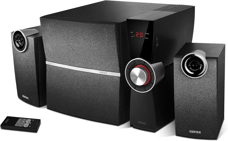 Edifier C2X
Testing the speakers
After cleaning the set a bit, I plugged it in and gave it a quick listen - immediately I could notice that the overall sound was pretty good and powerful, but the subwoofer's low-pass filter cutoff frequency was way too high for my preference. This could obviously just be the driver's characteristics, but testing with my previous Sony speaker proved that the LPF was simply configured weirdly.
As a totally scientific experiment, I took several measurements of the frequency response that the analog circuits in the C2X create. I used my PC's sound card for capturing line-level audio (after verifying that its own frequency response was a fully flat line). For the satellite speakers it was relatively easy, since they had a shared GND connection with the rest of the circuit, but the subwoofer output used a bridged (BTL) configuration, which meant I had to disassemble the amplifier and tap right before the TDA7379 power amplifier (as I didn't have a line-level converter yet).
I found the REW software which (among many other features) could plot a frequency response chart captured from a line input. On the below image, the blue line is my old low-pass filter I've been using (let's call it A-140), and the purple line is the C2X's filter.
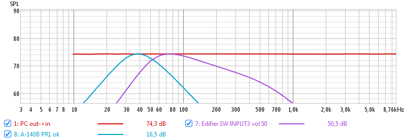 Comparison of frequency response
Both subwoofer filters also had a high-pass filter (probably to prevent the sub from receiving DC). Here's a comparison table:
| Filter |
High-pass filter |
Low-pass filter |
| A-140 |
27 Hz, 12 dB/octave |
57 Hz, 12 dB/octave |
| C2X |
49 Hz, 12 dB/octave |
100 Hz, 12 dB/octave |
As for the A-140, its LPF was adjustable (between 50-140 Hz), so the 57 Hz indicated was just what I used for my usual setting. The HPF was fixed at 33 Hz, per the manual (which measured close enough, no circuit is 100% ideal).
What to do with an amplifier that doesn't sound as expected? Disassemble it and try to find ways to modify it, for example.
Disassembly and initial lookaround
 Inside of the amplifier unit (forgot to take a photo, sorry)
The whole system seemed tidy inside - there were just 4 PCBs in total, and a power supply. The lower-left board had an audio EQ processor (TDA7303) and a 4-channel power amplifier (TDA7379). Oddly enough, it was a class AB amplifier - I would have expected a D-class here. Two of the IC's channels were used for the left and right satellites, and the other two were bridged to output to the subwoofer.
The TDA7303 chip has three stereo inputs and four outputs, since it's made for car radio applications (and most cars have four speakers). It supports volume and basic tone control, as well as per-speaker attenuation (this is most likely how bass level adjustment is done in the C2X).
What also caught my attention was an STM8S003 microcontroller on the display board - heck yeah, a programmable speaker set? Sounds cool - even if the IC was locked down (or OTP?), I had a few spare ones that I could simply swap.
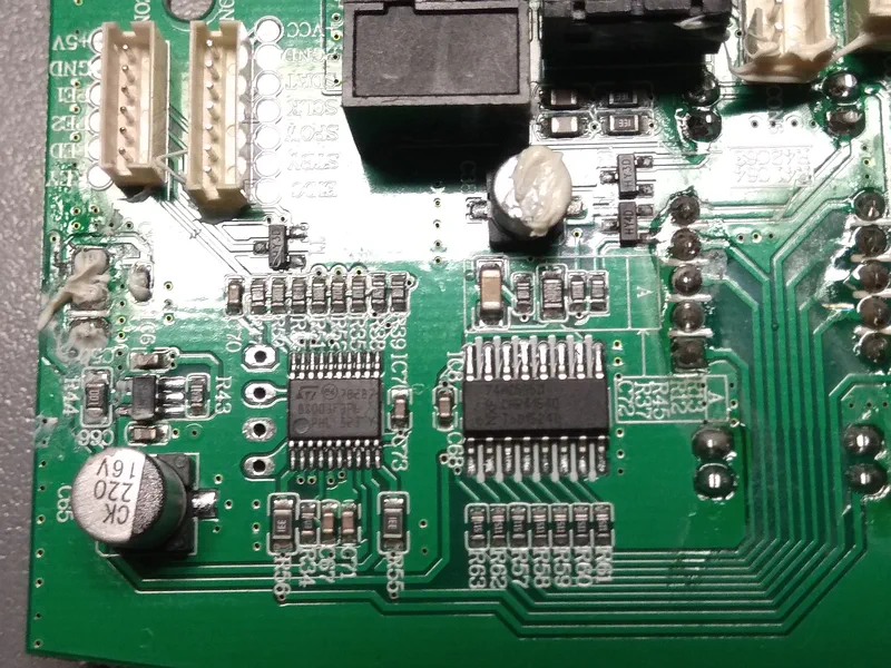 STM8S003 microcontroller
Still, my reason to be there was to inspect and modify the audio filters on that main board. To understand the circuit, I decided to try reverse-engineering the board.
Reverse-engineering PCBs
Previously I have tried the PCB Tracer software. It's a browser-based tool which allows to load photos of the top & bottom layers of a PCB, and then visually lay down all the traces, vias and components. Just like you'd do in CAD, but with a photo below and some other useful features (such as using AI to generate a schematic out of this).
While the tool seemed really cool, I found it pretty cumbersome to use. Without diving too deep into details, here are some issues with the current version:
- It was generally very buggy. Components couldn't be moved by dragging (only arrow keys), but they would instead randomly move when editing the pin assignments.
- There was absolutely no way to crop the photo or rotate it permanently. I took a photo with some extra stuff on the edges (and rotated by 90 degrees), and the only way was to change the view of the images, which made all components display sideways. Oh, and it resets every time I loaded the project.
- There was an option to set the PCB dimensions in mm/inches, but that dimension wasn't even used anywhere. I couldn't scale the initial photo to make the coordinate system correct.
- It's not open source. And I have a feeling a lot of AI was used to create it.
One of the main upsides was a really good landmark alignment utility. Selecting 4-8 points on each of the layers (such as vias, mounting holes or component legs) made it transform and align them perfectly.
I've also tried pcb-tracer (a different project), which feels more friendly to use, but it's too basic for performing a complete reverse-engineering of a PCB.
This time around, however, I wanted to try KiCad - the EDA software that I already was well familiar with (after switching from good old EAGLE, R.I.P. thanks to Autodesk). KiCad supports including bitmaps and images into a PCB file for reference. I could then draw a board outline (using the exact measured dimensions) and start adding components (with real-size packages), drawing traces, etc.
But before doing that I needed a perfectly-framed photo of both PCB layers. KiCad can't transform images using landmarks, so I needed another piece of software to prep the photos first. Oh, correction - I needed to take them first.
Taking photos, how hard could it be?
I used my cheap digital microscope to take around 40 pictures of the board - being a microscope, it can't just take one big picture of the entire PCB. Why not just use my smartphone or another camera, you may ask? The microscope has a stand that's mounted to the metal bed - placing the PCB on it flat should result in (mostly) straight-down photos, and helps maintain the same perspective when taking all photos.
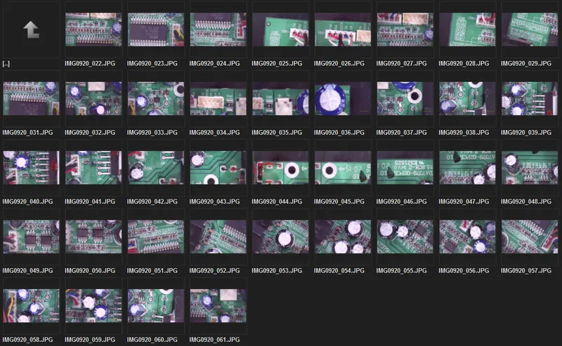 Thumbnails of all taken photos (top layer)
To stitch the images together (kind of like a panorama), I used Hugin, which is a panorama stitching tool, developed since 2003.
Using their scanned images stitching tutorial and some trial and error, I managed to create a complete representation of the board using the following workflow (version 2025.0.1):
- Enable Expert mode.
- In
Photos -> Geometric select Custom parameters.
- Launch the
Fast Panorama Preview (Ctrl+Shift+P). Set Projection to Rectilinear.
- Add one image in
Photos tab.
- Add a new image that overlaps with what's already added.
- For any new images, set their
Roll in Optimiser tab (measure the angle first).
- Go to
Control Points, choose the latest image in the right pane.
- Go through all images showing the same area in the left pane. Press
Create cp for each pair (change from Celeste using right mouse button).
- Inspect the created control points for each of the image pairs, remove any incorrect matches.
- In
Optimiser tab unselect all Yaw, Pitch checkboxes, select all except first for X, Y and Z. Click Optimise now!. It might get a little confused when optimizing all images at once, so it helps to run it incrementally. Hiding images from the preview can be used to ignore particular ones.
- Repeat steps 5-9 by adding photos for more of the missing areas.
- In the preview window, go to
Move/Drag. Set Drag mode to mosaic, click Centre and Fit. Adjust the image if needed.
- Crop the image as desired using the
Crop tab.
- Go back to the main window, in
Stitcher press Stitch!.
I found that it was best to stitch the PCB's boundaries first, then complete the inner parts. Getting a nice, straight outline was the most important part to achieve a good result. Also, an important rule - never put control points on tall components (like THT parts or connectors). The perspective will distort the result so badly, that it won't be able to keep the correct scale of the photos.
At some point I also created a PNG file, containing a rectangle with the PCB's dimensions (70x69 mm), like this:
 Image with a green rectangle resembling the solder mask outline
Matching control points between this rectangle and photos showing the PCB corners made the result adhere to the dimensions much better. I only had to disable this image during stitching (but after optimizing), otherwise the rectangle would cover all the other photos.
And then I gave up with this idea. Here's the best I got - from two separate incomplete attempts:
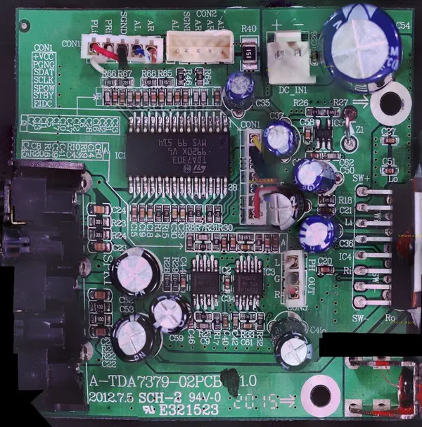 Stitched image using automatic Roll
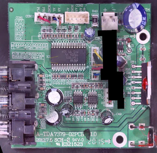 Stitched image using manual Roll
Clearly, the second method (with manual angle calculation - described above) worked better, but it still turned out to be far from usable.
TL;DR: eventually I took a few photos using a DLSR camera positioned ~1 meter above the board, in a tripod, with maximum possible zoom, manual focus, and some LED lights to make sure the board was evenly lit. Then I combined the photos manually in GIMP (the PCB has soldered-in wires, which I had to move out of the picture to uncover more area).
And here's the result from GIMP, after no more than 30 minutes of editing - for both top and bottom layers, perfectly aligned and scaled. I exported both layers with 30 px/mm resolution (though it's half of that on this site).
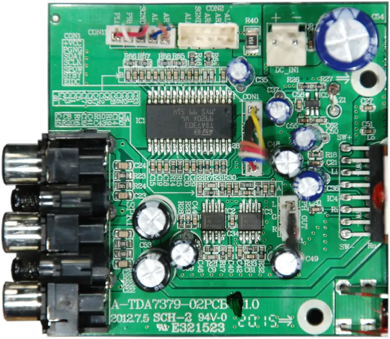 Top layer
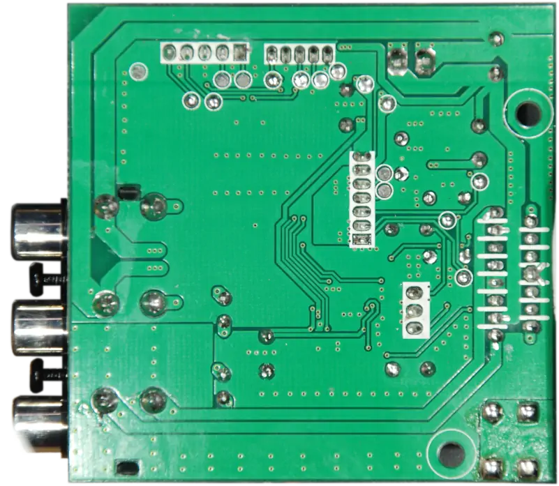 Bottom layer
Now I could finally start reverse engineering this board!
(Re)drawing a PCB in KiCad
Using the Insert -> Add reference image tool I could insert the JPEG into the PCB editor. It's possible to scale the inserted image, which had to be done - a JPEG imports at 300 PPI by default, which is around 11,81 px/mm, so a scale of 0,394 had to be used.
KiCad isn't really designed for reverse-engineering - the schematic is usually the source of truth - so I had to be a little creative. First, I placed all of the SMD and THT components on the top layer. This was relatively straightforward, given that the image was scaled properly, so I just had to rotate and align them with the background.
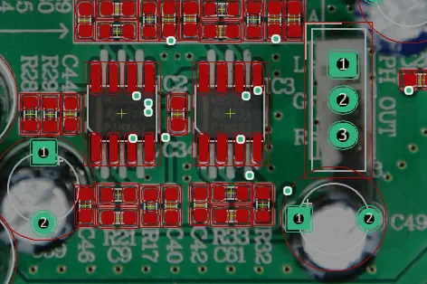 Components placed on top of the photo
Next, I assigned a name to each of the components - thankfully, they were labeled on the original PCB. After creating the respective symbols in the schematic, the footprints were connected - this wouldn't be needed if my goal was to just draw the traces, but I wanted to recreate the schematic (at least partially). One caveat with this method is that I couldn't connect traces between components, because it would create a net conflict. To make this possible, I had to connect the components in the schematic editor first, then draw traces.
Overall, after a few hours I had a complete, reverse-engineered schematic of the original amplifier board. Check this out:
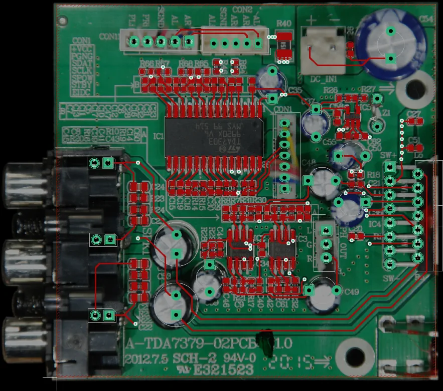 PCB top layer with components in KiCad
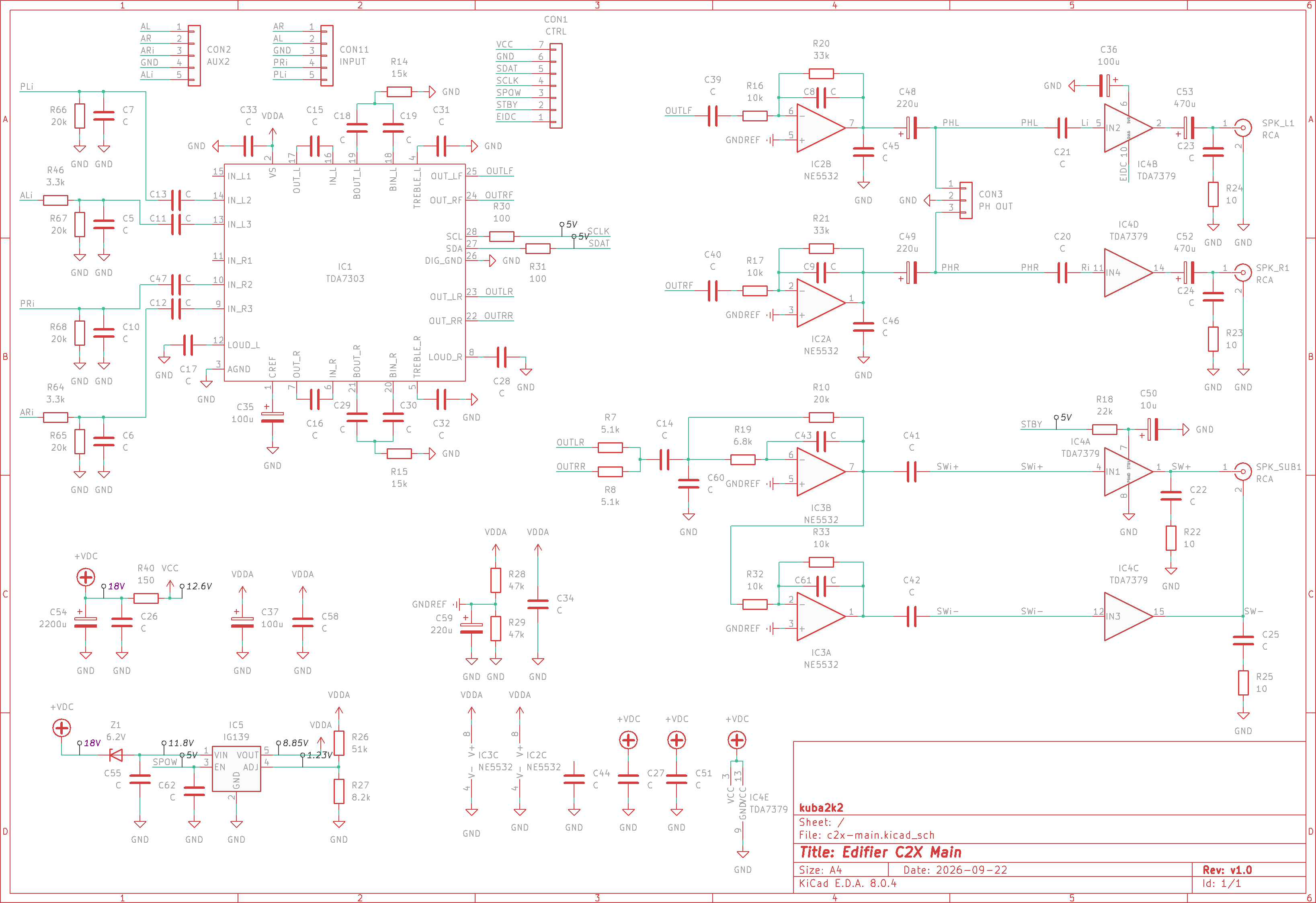 Reverse-engineered and cleaned-up schematic in KiCad
Understanding the circuit
At first glance, the entire schematic seemed really simple and easily understandable. It consisted of a couple main blocks:
- power regulator, bringing the 18V input down to about 9V for the analog parts,
- input stage with
TDA7303 audio processor (3x stereo inputs, one unused, and 4 output channels),
- left/right speaker filter stage (
NE5532),
- subwoofer filter and inverter stage (
NE5532),
- output power amplifier (
TDA7379) in stereo+bridge configuration.
At this point, my main goal was to modify the subwoofer filter - decrease both its LPF and HPF cutoff frequencies. I didn't know the capacitor values yet (since it's not possible to measure them in-circuit), and the IC3B op-amp configuration seemed complicated, and I couldn't work out what it did from just the schematic.
To aid debugging, I did a few more frequency response measurements using REW at various points in the circuit's audio pipeline. I made a few interesting observations.
- Both PC and Aux inputs had the same response, even though Aux had a slightly lower level (
R46+R64 before TDA7303).
- There was no change in
TDA7303 configuration when headphones were plugged in.
- Capacitors
C13/C11/C47/C12 formed an HPF, even before entering the TDA7303. That one was already cutting off anything below 23 Hz.
- All outputs from the TDA7303 had a predefined bass boost applied at around 72 Hz (around +5 dB).
- There was a second HPF built with
C39/C40, with cutoff frequency of around 50 Hz. That was being fed to the headphone jack.
- The final HPF for left/right speakers was
C21/C20, at around 180 Hz.
- For the subwoofer part,
IC3B added an HPF at 92 Hz, and there was another one at 100 Hz somewhere it seems.
The most confusing part was the bass boost enabled at all times. Previously I thought it was only applied when headphones were plugged in, but that turned out to be wrong. This made all measurements harder to understand, because the entire pipeline relied on an already-modified output from the TDA7303.
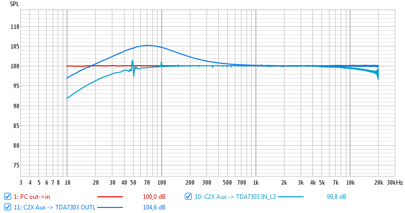 Bass boost on the OUTLF output
Since it was all controlled by the STM8S003 microcontroller, there must be just a command sent to the TDA7303 to enable bass boost. If only I could disable it...
Reprogramming the MCU
The engineers were kind enough to label the SWIM programming port on the display board. The STM8S offers some security measures against reverse-engineering, for example readout protection. To my surprise, I could read the entire memory using an ST-LINK V2 clone:
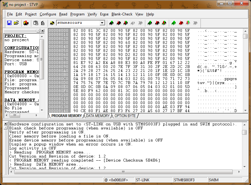 ST Visual Programmer dumping program memory
Using something called gmtdisas I could convert the resulting .hex file into assembly instructions:
λ gmtdisas.exe -rel0 -ioname program.hex > program.asm
λ head program.asm
;-------------------------------------------------------------------------------
.area FLASH (ABS, CSEG)
;-------------------------------------------------------------------------------
.org 0x008000
            int   0x00813C                         ;0x008000,    82 00 81 3C
            int   0x00905F                         ;0x008004,    82 00 90 5F
            int   0x00905F                         ;0x008008,    82 00 90 5F
            int   0x00905F                         ;0x00800C,    82 00 90 5F
            int   0x00905F                         ;0x008010,    82 00 90 5F
            int   0x00905F                         ;0x008014,    82 00 90 5F
I had to adjust its bundled stm8.inc to add correct register definitions for the STM8S003, but other than this it seemed to do the trick.
To re-assemble the program, I used SDCC:
λ sdasstm8 -o program.asm
λ sdld -i program.rel
ASlink >> -i
ASlink >> program.rel
λ head -n 2 program.ihx
:208000008200813C8200905F8200905F8200905F8200905F8200905F8200905F8200905F0A
:208020008200905F8200905F8200905F8200905F8200905F820090608200905F8200905FB7
The resulting program was almost byte-identical to the dumped one (I had to correct one instruction). This meant modification of the original firmware was possible!
Looking at TDA7303's datasheet, the bass boost function was configured in 2 dB steps. The +5 dB I measured before was obviously just a rough figure, so it could either be setting +4, +6 or even +8 dB.
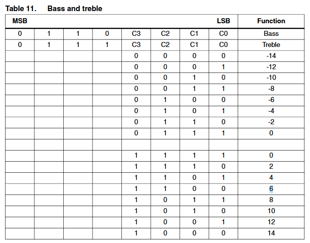 Bass/treble register datasheet
The respective byte values sent to the audio processor would be:
| dB |
Value |
Hex |
| +4 |
0110 1101 |
0x6D |
| +6 |
0110 1100 |
0x6C |
| +8 |
0110 1011 |
0x6B |
Searching through the disassembly revealed no matches for neither 0x6D nor 0x6C, but exactly one match for 0x6B:
ld    A, #0x3F
callr .+51  ;(0x008A67)
ld    A, #0x6B
callr .+47  ;(0x008A67)
Right! Assuming that 0x8A67 is the I²C write function, this piece of code would first write 0x3F, then 0x6B, setting the bass boost to +8 dB. But what could 0x3F stand for?
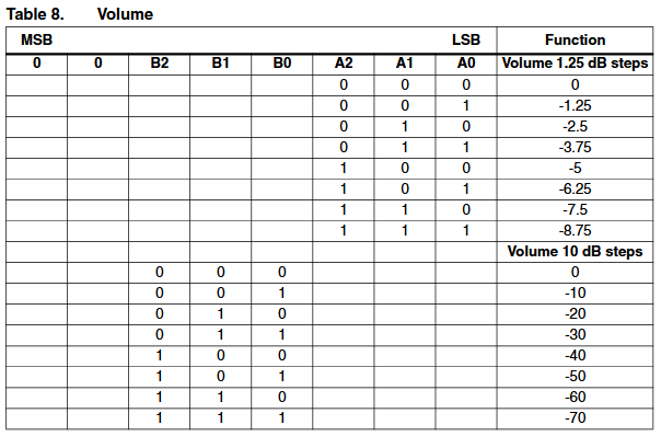 Volume control register datasheet
Sure, setting volume to -78.75 dB seems like a reasonable thing to do, perhaps as part of some initalization process. That meant I could modify this instruction to write, say, 0b01101111 (0x6F) to disable bass boost entirely.
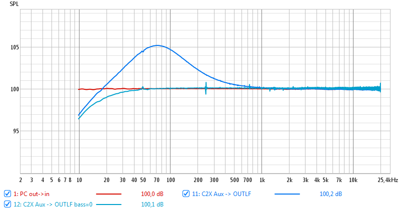 REW capture of OUTLF with modified firmware
Much better!
Inspecting the audio filters
Modifying the firmware was fun and all, but that alone wouldn't let me actually correct the frequency response of the subwoofer output. I still had yet to understand the high-/low-pass filter circuits, and it wasn't going to be easy with just the REW measurements. Instead, I decided to desolder the 0603 SMD capacitors, one by one, and test their capacitance out-of-circuit.
Desoldering was easy, provided I used enough extra solder, but soldering them back was painful enough. Normally when I assemble PCBs I use a solder stencil with solder paste, none of which were available here. Still, I managed to solder some of them back without making too much of a mess.
Why only some of them? Well, just because their values were so wrong, at least for what I was trying to accomplish.
Let's start with the input stage - capacitors before the TDA7303 (C13/C11/C47/C12). All of these measured around 510 nF, which combined with the IC's 50 kΩ input resistance would form a 6 Hz high-pass filter - my 23 Hz measurement seemed to disagree here. I didn't put these back on the PCB to replace them with 2.2 uF parts later on - this value should avoid cutting out anything in the audible frequency range.
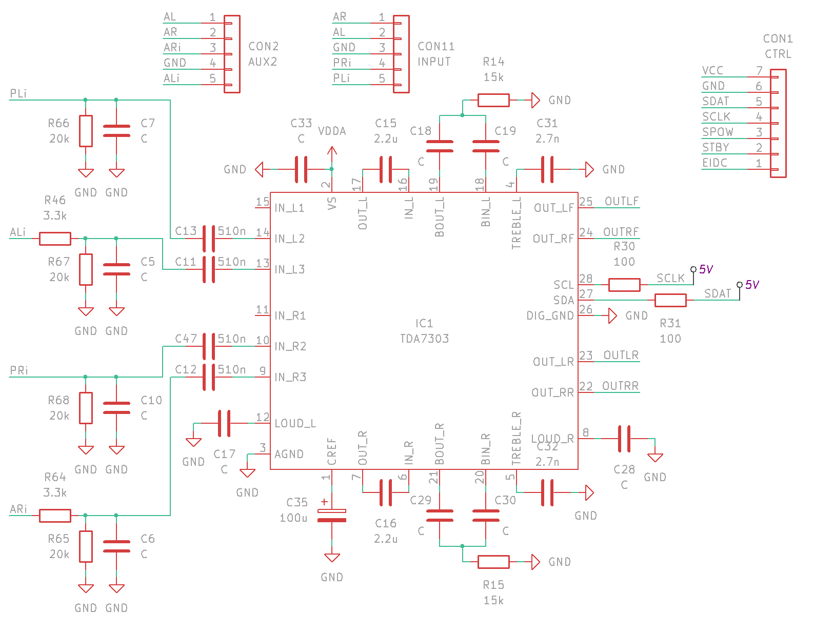 Schematic - input stage
Next, there's the C39/C40 high-pass filter, right before the left/right preamplifier. That didn't directly affect the subwoofer filtering, but it would still apply to the headphone output. Both capacitors measured 160 nF - not sure what the NE5532's input resistance is in this configuration, but measurements proved it was filtering at around 52 Hz. Not great, since I'd expect the headphone output to be as close to source as possible - hence I decided to install 2.2 uF capacitors here as well.
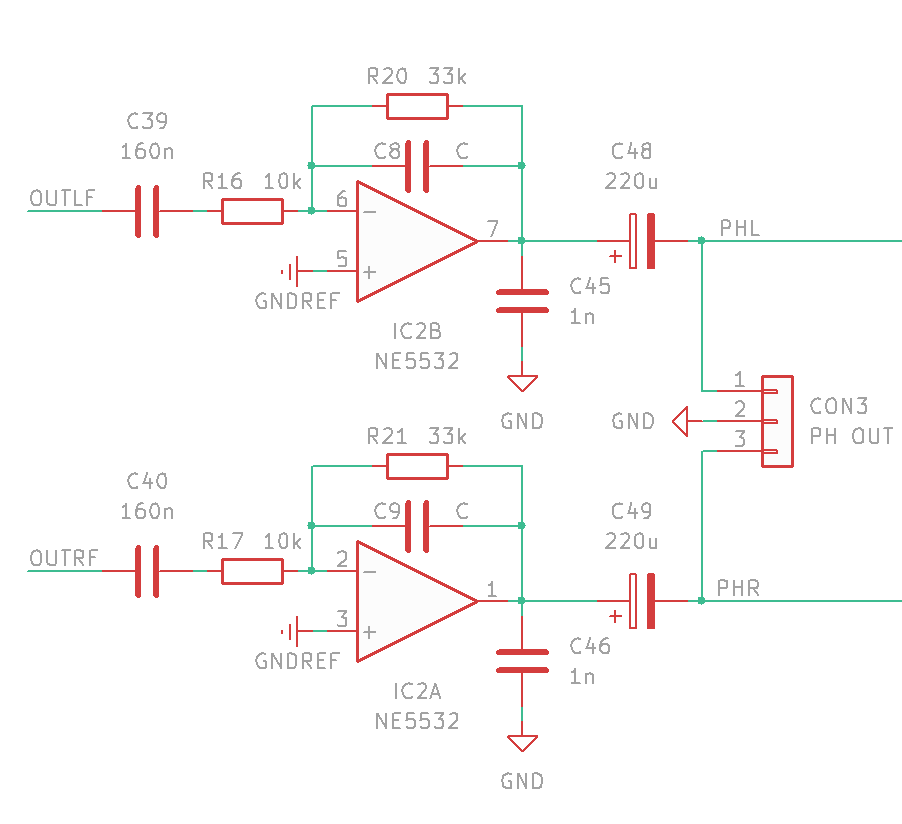 Schematic - left/right filter stage
Going further the left/right speaker audio pipeline, there was a filter made of C21/C20, both at 36 nF. With a typical input resistance of the TDA7379 at 15 kΩ, that would make a high-pass filter at 295 Hz, which should be fine for the small speakers.
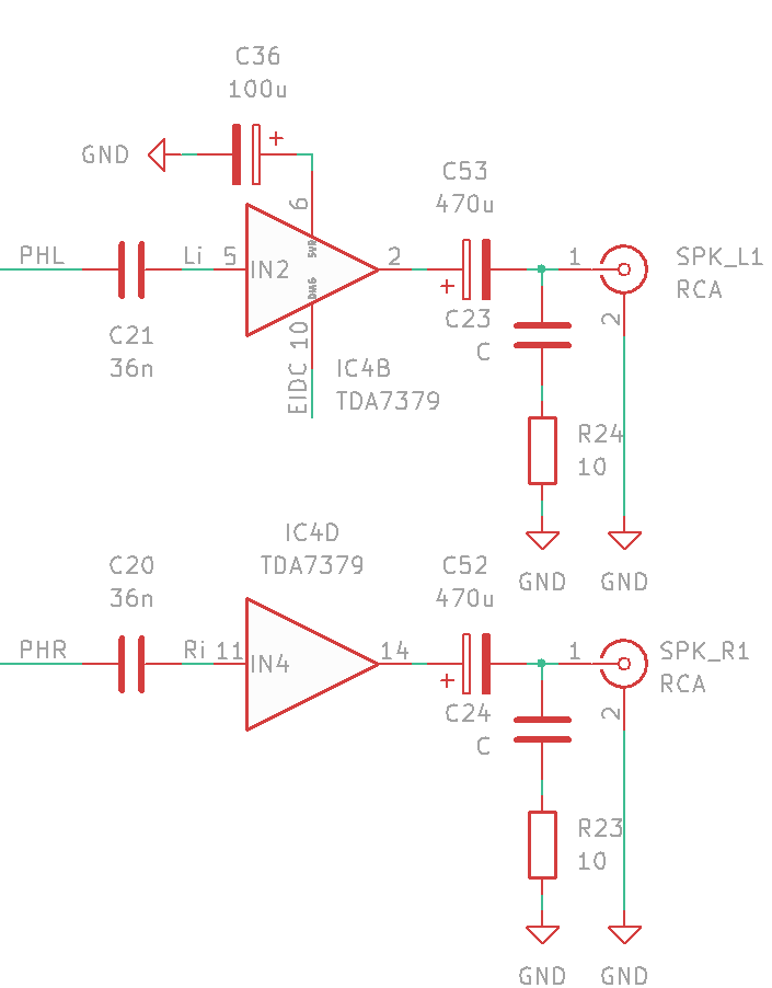 Schematic - left/right output stage
The subwoofer filter though... I was completely lost here. This wasn't any configuration I've seen before - though I'm far from an expert in analog electronics.
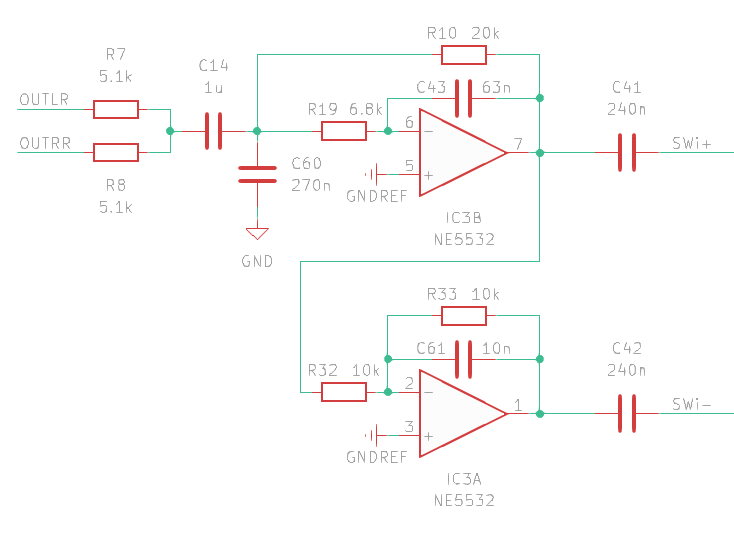 Schematic - subwoofer filter stage
I tried asking ChatGPT, but in all few attempts it gave me explanations that didn't make sense. But it did give me one important clue as to what this could be - a multiple-feedback low-pass filter.
Then I found a design tool for that type of filters - at OKAWA Electric Design website. Entering all exact values from the schematic finally gave me meaningful results:
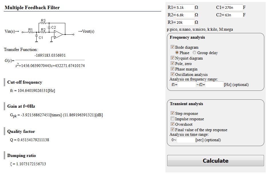 Multiple Feedback Low-pass Filter Design Tool
If I then calculated the output high-pass filter formed by C41/C42, I got 44 Hz at 240 nF and 15 kΩ. All this just happened to confirm my measurements:
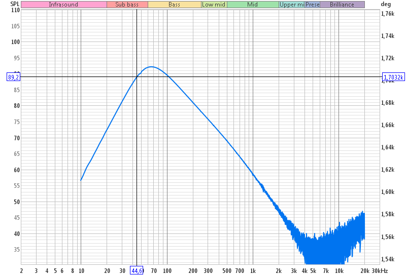 High-pass subwoofer cut-off frequency measurement
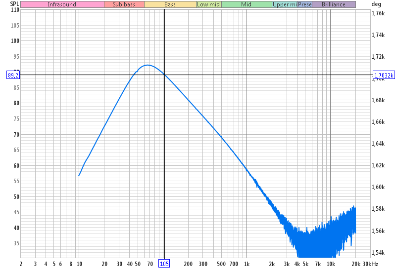 Low-pass subwoofer cut-off frequency measurement
Clearly, C41 and C42 also needed to be replaced with 2.2 uF parts. Why would they cut off the bass output like that? I needed all the bass.
After playing around with the design tool for a bit, I found that modifying R2 (R19=6.8k) value allowed changing the cut-off frequency without affecting the gain.
Seemed like a perfect opportunity to install a digital potentiometer!
Inspecting the control board
But first - I needed to find out if there were enough GPIOs usable on the control board to connect a digital potentiometer IC. Since I had a couple of MCP41100s at hand, I was looking for a way to connect an SPI device to the MCU.
Using a multimeter and manual PCB tracing, I created a GPIO map of the STM8S003 chip:
                 STM8S003F3P6
              +----------------+
  LED_AUX_PC -| PD4        PD3 |- KEY_ADC
        SHCP -| PD5        PD2 |- VOL_PE2
        STCP -| PD6        PD1 |- VOL_PE1
      RST_RC -| nRST       PC7 |- ---[/\/\10k/\/\]--- NPN --- KEY_LED
          DS -| PA1        PC6 |- ^HP_DET
       IR_RX -| PA2        PC5 |- ---[/\/\ 1k/\/\]--- EIDC
         GND -| Vss        PC4 |- ---[/\/\ 1k/\/\]--- STBY
         cap -| Vcap       PC3 |- ---[/\/\10k/\/\]--- SPOW
         +5V -| Vdd        PB4 |- SCL ---[/\/\10k/\/\]--- +5V
LED_BASS_TRE -| PA3        PB5 |- SDA ---[/\/\10k/\/\]--- +5V
              +----------------+
as well as the accompanying 74HC595 (for controlling the LED display):
                  74HC595
             +---------------+
      LED_F -| Q1        Vcc |- +5V
      LED_A -| Q2         Q0 |- LED_G
      LED_B -| Q3         DS |- PA1
      LED_C -| Q4        ^OE |-x
      LED_E -| Q5       STCP |- PD6
      LED_D -| Q6       SHCP |- PD5
  DIGIT_SEL -| Q7        ^MR |- +5V
        GND -| GND       Q7S |-x
             +---------------+
For the STM8S's nRST, there was a 10k pull-up resistor, as well as a pull-down capacitor installed - this provided a delayed startup to the MCU.
Now, the MCP41100 only needed three SPI pins - SCK, MOSI and CS. But there were no free pins remaining on the STM8S.
To get around this, I used a similar technique as in my old CDCEmu v2.1 project:
- The SPI's CS pin could be shared with I²C's SCL:
- during SPI activity, I²C will see a low clock and nothing on SDA, so nothing will happen,
- during I²C activity, SPI will see some pulses on CS, but nothing on the data/clock lines.
- The SPI's SCK and MOSI pins could be shared with
74HC595's SHCP/DS:
- during SPI activity,
74HC595's internal shift register will change, but lack of STCP pulse won't change it's outputs,
- during
74HC595 activity, SPI will do nothing because its CS will be high.
At least that was the theory. Assuming this could work, I had to work out how to connect the digital potentiometer to the low-pass filter.
Making the audio filter adjustable
As I previously mentioned, changing R19 allowed to adjust the filter's cut-off frequency. The MCP41100 is a 100 kΩ potentiometer, and its datasheet gives a formula for calculating the resistance at a given digital code (0-255).
If the potentiometer was to be used as a rheostat between its wiper and A terminal, the resistance ranges from 390 Ω (code 255) to 100 kΩ (code 0). Consequently, if used between the wiper and B terminal, the range is from 0 Ω (code 0) to 99.6 kΩ (code 255). In both cases, one step of the data value is 390 Ω. Since R2 value cannot be 0, the A-W arrangement could be used.
On sxlab.ru I found a second-order low-pass filter calculator, which gave me the necessary formulas for calculating the gain, frequency and quality factor:
$$f = \frac{1}{2 * \pi * \sqrt{R2 * R3 * C1 * C2}}$$
$$k = \frac{R3}{R1}$$
$$q = \frac{\sqrt{\frac{C1}{C2}}}{(1 + \frac{R3}{R1}) * \sqrt{\frac{R2}{R3}} + \sqrt{\frac{R3}{R2}}}$$
By some trial and error, I found that using C1=510nF and C2=27nF (and changing some neighboring resistors) gave quite satisfying results, allowing (way too) fine adjustment between 18 Hz and 50 Hz, and more coarse adjustment above that, all the way to around 300 Hz. The Q factor also seems to have improved from the original circuit's 0.452.
There was just one small problem with all of this. The MCP41100, just like most other digital potentiometers, could only accept Vss..Vdd on its A/B/W terminals. I needed to connect it in place of R19, which was connected to the op-amp's inverting input, kept at Vcc/2 by the IC - meaning around 4.5 volts. The input signal could go below or above that, so by powering the MCP41100 from 5V, only about 0.5V of headroom was left for the audio.
To make it easier to understand, let's suppose the signal was 2 Vpp at most - that could put one of R19's terminals at 3.5-5.5 volts - too much for the MCP41100 to accept.
I researched other methods for making a digitally-controlled resistance (MOSFETs, JFETs, VCOs, OTAs), but all of them were way too complicated to implement here. Instead, I came up with a truly cursed way to still use the digital potentiometer.
Hear me out, this will work...
Voltage is relative, right? The 4.5V at R19's terminals was relative to the circuit's GND, and that's why the MCP41100 couldn't interface with it directly. But who said its ground needed to be the same as the rest of the circuit's ground?
That's right - the 100% production-ready idea was to offset the MCP41100's ground by around +2V. Using the 2 Vpp signal example from before, this would shift R19's voltages to 1.5-3.5 volts above the 2V-ground, which would be perfectly acceptable for the potentiometer chip.
The plan was simple - create a new voltage reference using a 1.8V regulator powered from the 9V rail, then add another 5V LDO between that new GND and the same 9V rail. This would create a new 2V (more or less) line and a 7V one, keeping the audio signals mostly in between, while ensuring the MCP41100 got its rated 5V power input.
Okay then, but what about the SPI control lines? Sending 0V there would bring it to -2V - below the chip's Vss!
I needed a level shifter - but not a standard one. If I used an NPN transistor or a MOSFET, it would still be problematic to drive it with an offset voltage (and it would also invert the signals).
All these issues could be solved using an optocoupler - three of them, actually - for the three SPI data lines. Optocouplers provide galvanic separation between the "driving" side and the "receiving" side. The internal transistor is not activated by base current, but optically using a LED (or something) hidden inside of the package.
Sure, this will work...
I installed pull-up resistors on all three SPI lines on the MCP41100's side (to bring them up to +7V). The same lines were then connected to the optocouplers' collectors, and their emitters to the fake GND (+2V). On the "transmitting" side, I wired up all three anodes to +5V (of the MCU) via separate resistors, and the cathodes to chosen GPIO pins.
Simply - a logic HIGH level wouldn't activate the optocouplers, so their collectors stayed at the +7V pull-up. A logic LOW on each cathode would bring the collectors to +2V, so the digital potentiometer would see 0V.
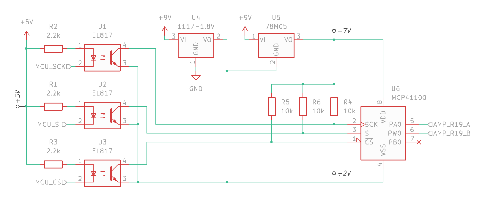 Schematic of the not-so-TTL level shifter
Armed with this wonderful idea, I assembled this on a prototyping board. After plugging it into +9V power, no magic smoke was let out, and the MCP41100's wiper measured around 45 kΩ - success! The chip was getting power, at least.
Probing further with a multimeter confirmed that Vdd-Vss was around 5V, and its ground was indeed around 2-3V above the real one. Since the STM8S003 MCU wasn't yet programmed to interface with SPI, I used an FT232RL adapter with my pyftdi-bitbang project to send SPI commands from my computer.
With a quick Python UI consisting of just a slider and a label with approximate filter parameter calculations, I could control the cut-off frequency digitally!
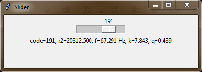 Filter control UI
Writing firmware
Without going too much into the details here, I ended up rewriting the entire STM8S003 firmware from scratch. It wasn't that difficult - I used a simple state machine in the main loop, that simplified the LED display menu system greatly.
I had some trouble getting both I²C and SPI to work on the same GPIO, but I managed to get it working by restarting I²C after touching SPI pins.
By the way of having custom firmware, I also added more settings to the menu, such as bass adjustment (not subwoofer level - different things!), satellite speaker attenuation, loudness correction and gain control. Overall, the result was really satisfying.
Here's a demo video, recorded with a webcam from 2012 - enable sound to hear it in action:
Who needs more than 6 frames per second?
In total, fixing up the subwoofer LPF required removing R19, and changing its surrounding components: R7/R8 to 22 kΩ, R10 to 68 kΩ, C60 to 510 nF, C43 to 27 nF, and C14 to 2.2 uF (just to have move the HPF lower).
Apart from that, I also changed the previously-modified C49 and C40 to 100 nF. I figured that the headphone output was useless anyway - there was no dedicated headphone amplifier, and NE5532 was too weak to drive even 16 Ω headsets. Also, at that impedance, C48/C49's HPF would have a -3 dB cutoff frequency of 45 Hz, not great.
But that wasn't even the primary reason - if I made IC2 output full-range sound, then the only HPF going to the satellite speakers were the two C20/C21 capacitors, both at 36 nF. The frequency was perhaps not wrong, but being a passive first-order filter, it had a pretty gentle slope. And keeping IC2 as it was from the factory also applied the HPF to the headphone output - also wrong. So I decided to just ignore that the output existed, and install 100 nF caps to drive the satellites a bit less hard.
Final calibration
Before reassembling the unit, I wanted to find the perfect settings to get the C2X sounding as close as possible to my previous setup - just because I was used to it, and it always satisfied my needs (in terms of sound quality, not how messy it was...).
Using a couple of relays I made a quad-pole/dual-throw switch - yeah, I know it sounds made up. Basically, the following circuit:
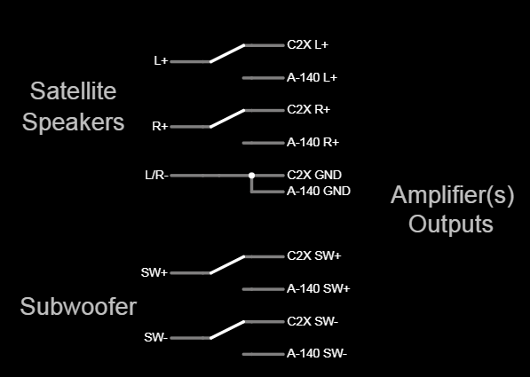 Amplifier->speaker switch board
The satellite/subwoofer relays were individually controllable, so I could select each of the two amplifiers freely. Since subwoofer outputs use a PBTL configuration, using a common GND wasn't possible, hence two relays for that one speaker.
Using REW again, I captured a frequency sweep using each of the 4 possible configurations, in order to adjust the subwoofer level and LPF cut-off frequency in the C2X to match the ones from A-140. Then, by quickly switching between amplifiers while playing some music, I could verify that they sounded mostly the same (at least the subwoofer part).
Here's a comparison graph - green traces are the A-140, yellow traces are the Edifier amplifier after modifications. All captures were made on the speaker outputs (using a line-level converter), with speakers disconnected.
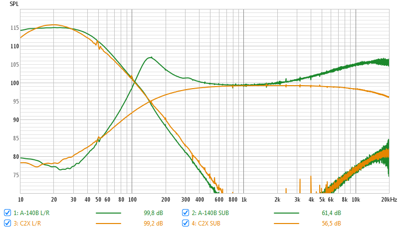 Comparison of two amplifiers on two outputs
The subwoofer filtering turned out to be pretty much spot on. As for the satellites... apparently my Cambridge SoundWorks set had a built-in bass and treble boost, for some reason. But now I wanted it on the C2X too - without that, the sound was just flat.
Treble adjustment was built into the TDA7303, but the default 2.7 nF capacitor was way too large - setting treble boost to even +6 dB pretty much boosted the entire mid frequency section. I ended up having to replace the C31/C32 capacitors with 1 nF ones - that made the result way better indeed.
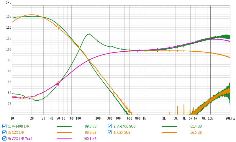 Pink trace - treble boost +8 dB
I decided to leave out my original setup's bass boost, since it wasn't really reproducible by the tiny satellites anyway. Also, here's a comparison of several treble boost settings, from 0 dB to +10 dB - for no reason, I just thought it looked cool.
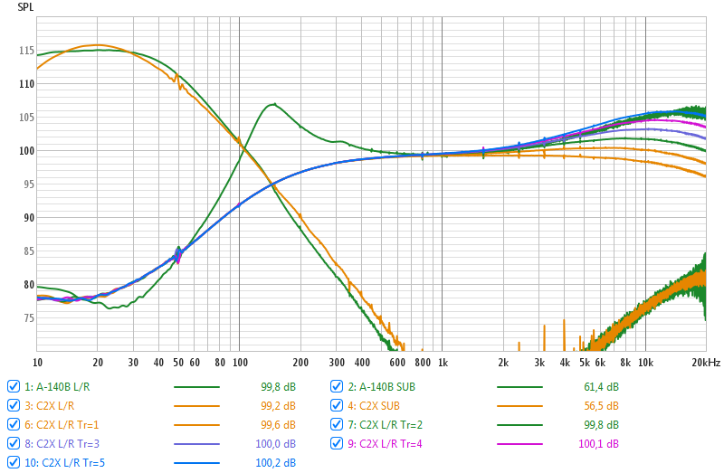 Colorful! And kind of nice
What about that drop at >=10 kHz? Okay, okay... yeah I could probably address that too. I thought it could be caused by the NE5532 feedback capacitors (C8/C9) acting as a low-pass filter, since the TDA7303's output response was perfectly flat, and the drop was only noticeable after the op-amp. That turned out to be wrong, removing these capacitors made no difference. As this has taken me way too long anyway, I decided to ignore this "issue" instead.
The result
All in all, I think the hardware modifications turned out pretty well. Here are a couple of photos from the finished build - including the custom perfboard with a digital potentiometer, a couple of volume regulators, and a mysterious module...
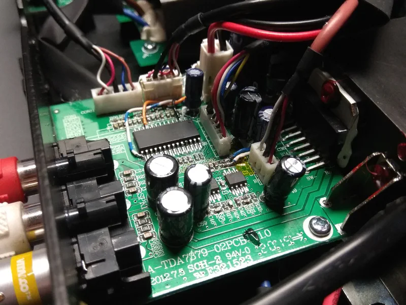 Main board modifications
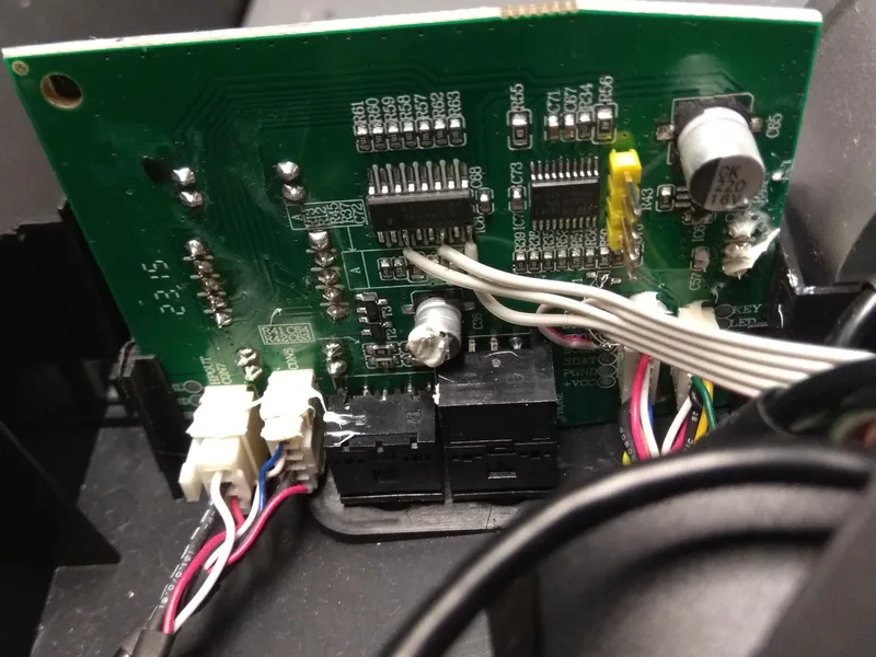 Control board modifications
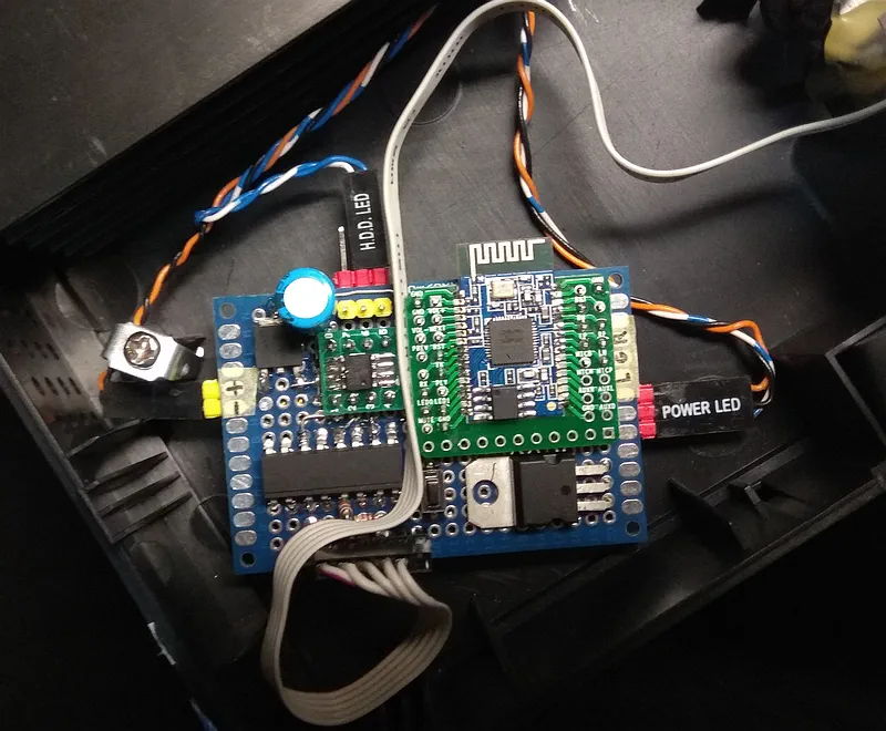 Custom prototyping board
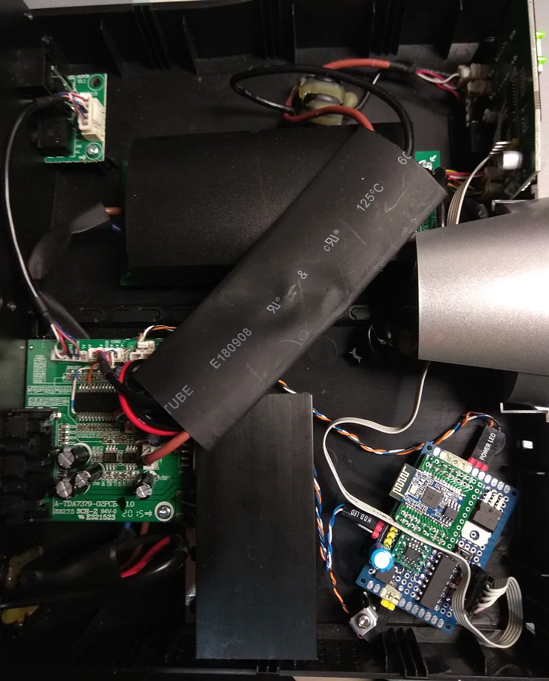 (Almost) assembled unit
About that module... because the TDA7303 had an unused INPUT_1, I added a Bluetooth receiver module to make the set wireless!
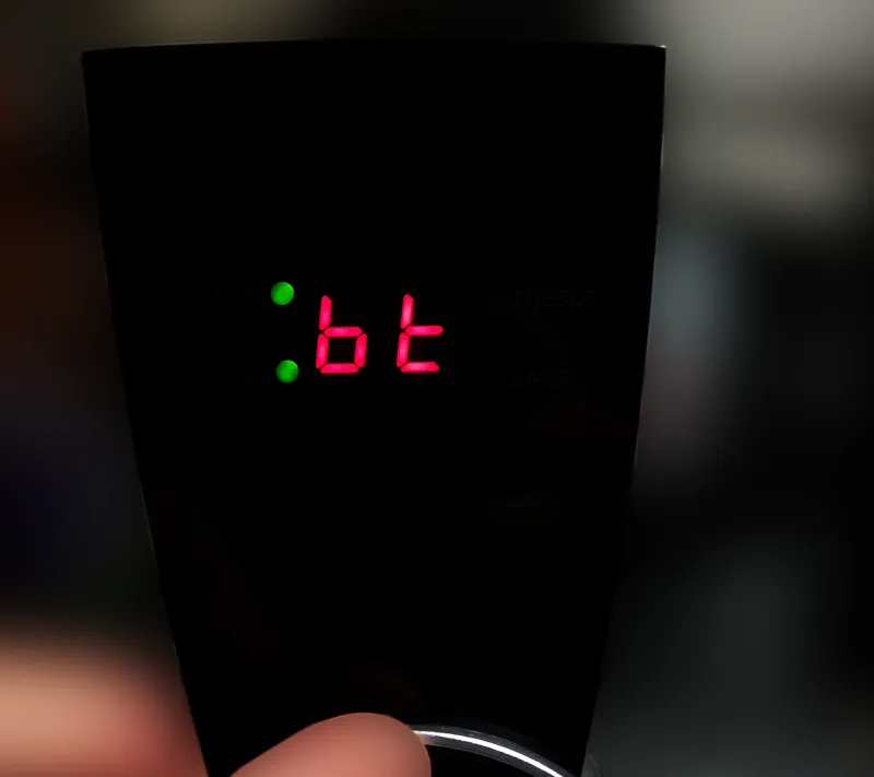 Bluetooth option on the LED display