This is a continuation of IPTV Reverse-Engineering - Part 1, right from where I left off.
And where exactly was that?
Oh, right... permanently destroying the device by lifting off the NAND flash chip.
 No hope left here
Note that this is still a backstory. As I'm writing this, it's October 2024, but I feel like the previous discoveries from 2023 shouldn't be left out if I want the story to be complete.
I may not have good photos for many parts of this story, because I didn't ever expect wanting to publish it anywhere.
Let's recap:
- the box was running the Linux kernel with U-Boot,
- there was no datasheet for the particular MStar MSO9380 chip,
- there were two pin headers on the PCB, with no signs of life on them,
- I found sources of U-Boot and MStar's
mboot on GitHub,
- Roku provided GPL sources of Linux and U-Boot on their website,
- I desoldered the NAND chip from the device using a hot air gun.
Note
This article is written for informational and educational purposes only.
Hacking into any kind of online service is NOT the point of this article, is by any means NOT condoned by the author of this post.
Breaking of DRM protection is also not the goal of this project and is considered illegal, as in piracy or theft.
No illegal activities related to hacking of any 3rd party service will be described in this article.
Building a NAND programmer
Anyway - having a raw NAND chip desoldered from the set-top-box, I needed to figure out two things:
- What am I going to connect it to? How am I going to connect it?
- How am I going to dump the firmware from the flash?
Unfortunately BGA sockets cost more than I was willing to spend on this project, so the obvious idea was... soldering it to a Raspberry Pi Pico with really tiny wires.
I started by looking at the pinout from the datasheet:
 NAND pinout with N/C pads removed
The bare minimum should be 4 Vss wires, 4 Vcc wires, 8 data signals, RE#, WE#, R/B#, CE#, WP#, ALE, CLE.
A not-so-quick soldering session later:
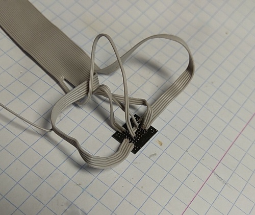
 NAND chip soldered to a ribbon cable
I used a ribbon from an old Enhanced-IDE cable, since the wires had a single core and were pretty thin.
For connecting to the Pi Pico, I added the female ending from the IDE cable and some male-to-male wires, since my Pi had female headers.
It sounds just as complicated as it looks. It is a mess of wires. But it was not supposed to look pretty, it was supposed to work.
 A mess of wires
(Yes, I didn't care enough to use anything else than a breadboard. Sorry for that.)
Writing a NAND programmer
With the hardware part pretty much ready, it was time to write some software for the Pi Pico. My first attempt was, obviously, reading the chip ID and printing it over UART (or, virtual USB serial port). I just needed to understand the diagram from the datasheet:
 ID Read waveforms from the datasheet
On the Pico, I prepared a few GPIO macros, some busy loops for timing, as well as some helper functions:
Macros and some helper code
#define nand_enable()  gpio_put(PIN_CE, 0)
#define nand_disable() gpio_put(PIN_CE, 1)
#define nand_cle_set() gpio_put(PIN_CLE, 1)
#define nand_cle_clr() gpio_put(PIN_CLE, 0)
#define nand_ale_set() gpio_put(PIN_ALE, 1)
#define nand_ale_clr() gpio_put(PIN_ALE, 0)
#define nand_we_set()  gpio_put(PIN_WE, 0)
#define nand_we_clr()  gpio_put(PIN_WE, 1)
#define nand_re_set()  gpio_put(PIN_RE, 0)
#define nand_re_clr()  gpio_put(PIN_RE, 1)

#define nand_pause()                                                                                                   \
    do {                                                                                                               \
        sleep_us(1);                                                                                                   \
    } while (0)
#define nand_wait()                                                                                                    \
    do {                                                                                                               \
        nand_pause();                                                                                                  \
    } while (gpio_get(PIN_RB) == 0)

void nand_dir_out(uint8_t value) {
    for (int i = 0; i < 8; i++) {
        gpio_set_dir(IO[i], GPIO_OUT);
        gpio_put(IO[i], (value >> i) & 1);
    }
}

void nand_dir_in() {
    for (int i = 0; i < 8; i++) {
        gpio_set_dir(IO[i], GPIO_IN);
    }
}

void nand_write_command(uint8_t value) {
    nand_cle_set();
    nand_we_set();
    nand_dir_out(value);
    nand_we_clr();
    nand_pause();
    nand_dir_in();
    nand_cle_clr();
}

void nand_write_address(uint8_t value) {
    nand_ale_set();
    nand_we_set();
    nand_dir_out(value);
    nand_we_clr();
    nand_pause();
    nand_dir_in();
    nand_ale_clr();
}

uint8_t nand_read() {
    nand_dir_in();
    nand_wait();
    nand_re_set();
    nand_pause();
    uint8_t value = 0;
    for (int i = 0; i < 8; i++) {
        value |= gpio_get(IO[i]) << i;
    }
    nand_re_clr();
    return value;
}
With this, I could try to read the chip ID:
uint8_t id[5];
nand_enable();
nand_write_command(CMD_ID_READ); // 0x90
nand_write_address(0x00);
id[0] = nand_read();
id[1] = nand_read();
id[2] = nand_read();
id[3] = nand_read();
id[4] = nand_read();
nand_disable();
printf("ID1=%02x %02x %02x %02x\n", id[0], id[1], id[2], id[3]);
After a few attempts, it worked! Sort of...
 A couple of ID readouts
The correct ID should be c2 dc 90 95, so the first readout was fine. After that, it seemed to drop the 2 least-significant bits. I suspected loose wires or timing issues - I haven't added any delays, I assumed the Pico was slow enough.
I was too lazy to connect a logic analyzer (no, it's totally not that the only "logic analyzer" I had was the very same Pi Pico...), so I just added a few 1 microsecond delays. And it worked!
 More ID readouts
The following day, I wrote a simple page reading snippet - it reads 2112 bytes (2048 + OOB data) from a specified address:
uint32_t buf_addr = 0;
uint8_t buffer[2112];
printf("Enter 1st address: ");
scanf("%hhu", &addr[0]);
printf("\nEnter 2nd address: ");
scanf("%hhu", &addr[1]);
printf("\nEnter 3rd address: ");
scanf("%hhu", &addr[2]);
printf("\nEnter 4th address: ");
scanf("%hhu", &addr[3]);
printf("\nEnter 5th address: ");
scanf("%hhu", &addr[4]);
nand_enable();
nand_write_command(CMD_READ_1);
nand_write_address(addr[0]);
nand_write_address(addr[1]);
nand_write_address(addr[2]);
nand_write_address(addr[3]);
nand_write_address(addr[4]);
nand_write_command(CMD_READ_2);
nand_wait();
buf_addr += 2112;
nand_write_command(CMD_CACHE_READ_SEQ);
nand_wait();
for (int i = 0; i < 2112; i++) {
    buffer[i] = nand_read();
}
nand_disable();
hexdump(buffer, 2112, buf_addr);
With this, I was able to retrieve the first page of the NAND:
000000  4d 53 54 41 52 53 45 4d  49 55 4e 46 44 43 49 53  |MSTARSEMIUNFDCIS|
000010  05 c2 dc 90 95 56 00 00  00 00 00 00 00 00 00 00  |.....V..........|
000020  9a 00 00 00 40 00 00 08  40 00 00 10 00 00 00 00  |....@...@.......|
000030  02 00 14 00 0a 07 10 14  46 00 3c 00 3c 00 00 00  |........F.<.<...|
000040  4d 58 49 43 00 00 00 00  00 00 00 00 00 00 00 00  |MXIC............|
000050  4d 58 33 30 4c 46 34 47  31 38 41 43 00 00 00 00  |MX30LF4G18AC....|
000060  00 00 3c 00 0f 00 00 00  14 00 0a 07 00 00 00 00  |..<.............|
000070  00 00 00 00 00 00 00 00  00 00 00 00 00 00 00 00  |................|
000080  00 00 64 00 00 00 00 00  00 00 00 00 00 00 00 00  |..d.............|
000090  00 00 00 00 00 00 00 00  00 00 00 00 00 00 00 00  |................|
0000a0  00 00 00 00 00 00 00 00  00 00 00 00 00 00 00 00  |................|
[...]
...which seemed to represent the Chip Info Structure (CIS) - I found a page about that on linux-chenxing.
The readouts weren't perfect at first - it was dropping some bytes at the end of each block. Sometimes it took more than 10 tries to read a single page correctly. Since it seemed to depend on the page's contents, I suspected some interference on the (relatively) very long, unshielded wires (duh!).
Then I added a 5.6 pF capacitor on the RE# line - Read Enable, which fetches the next byte to read, which could explain it causing dropped bytes. It was all perfect after that. Then I removed the capacitor, and it was still perfect. I never found out what was wrong before that.
With a serial terminal, I poked around the flash manually to find anything interesting, and at least I found strings and ARM code - that meant the NAND flash wasn't scrambled! I kind of expected that, since it was an SLC chip, but the fear of having to battle NAND scrambling was still somewhere in me.
 Strings visible in an UART terminal
A quick Python script later...
 Automated reading of all pages
Of course, there were still bitflips on some of the pages - I couldn't fix that issue. I ended up reading the image a few times, then trying to eliminate the differences. It was all painfully slow - after even more added delay()s, it was reading at a whopping 46 KiB/s.
I was inspecting the resulting file as it was reading, and found the U-Boot banner:
U-Boot 2011.06-00074-g09ea5d7 (Dec 05 2018 - 11:58:03)
Sadly, I also noticed a lot of TEE references and some PlayReady certificates - I hoped this was for the DRM stuff, not for firmware encryption. But anyway, I continued the flash readout via UART.
It took over 3 hours to read 512 MiB of data.
Exploring the firmware dump
With the complete image, I started exploring it in a hex editor. That, as well as searching for strings revealed a couple of interesting things:
- U-Boot environment variables (and the U-Boot itself)
- a firmware upgrade file URL (which I downloaded, obviously),
- no obvious signs of the Linux kernel in its usual form,
- UBI volumes and UBIFS filesystems,
- SQLite databases for Chromium local storage,
- more certificates,
- Wi-Fi credentials and user settings,
- and funny cats.
 Literally the image that was linked in the firmware dump
I was able to label the following partitions/images in the firmware - these were manually named by me:
00000000_cis1.bin
00020000_cis2.bin
00040000_unknown1_copy1.bin
00060000_unknown1_copy2.bin
00140000_unknown2_copy1.bin
00180000_unknown2_copy2.bin
001C0000_mboot.bin
00420000_mbootbak.bin
006A0000_ubild.bin
00840000_optee.bin
00E40000_armfw.bin
01000000_param.bin
01010000_tee.bin
01020000_loader1.bin
041A0000_loader2.bin
076E0000_splash1.bin
07B00000_splash2.bin
07F20000_download.bin
14E00000_ubi.bin
(the 1 and 2 bins were just byte-exact copies, possibly for backup purposes - it's a NAND after all).
cis was the NAND info block, with partition offsets, block sizes etc,ubild was the uboot .env (although referred to as "bootlogo" partition; there's no logo there anyway),optee and armfw were probably some TEE things,param had the model name, serial number, MAC address of the box and some unknown data,tee had a .TAR file with some widevine stuff,loader was nearly 40 MiB in size, probably the kernel and ramdisk, I assumed,download seemed to have some unknown data (in a format similar to loader), a "high level download" string at the beginning, a copy of mboot, and was around 140 MiB in size,splash had a boot logo (in JPG format) along with some U-Boot commands that display it,ubi was spanning the rest of the NAND, which had userdata storage only.
The loader and download images were probably the most interesting. Here's a hexdump of one of them:
The blank 0x00-filled spaces in the middle suggested that it wasn't encrypted (however, it could just be an image made of several encrypted parts). The 3 bytes before the blank spaces looked like zlib headers, but I couldn't get a good match (from a quick "magic byte" lookups on the net).
One thing worth noting is, I have checked the mboot sources that I got online, and found absolutely no mention of that image format.
I was able to extract the UBIFS partition with something called ubireader (a Python script). Previously, I tried nandsim in Linux, but that didn't work - presumably because of bad blocks or other issues alike. The UBIFS only contained user data - Wi-Fi config, Widevine certificates, Chromium cookies and local storage - no binaries or applications.
I have also tried binwalk (it was the first thing I did) but it could only identify the UBI volumes.
Disassembling the bootloader
It was time to disassemble the U-Boot binary. To no surprise, it turned out to be heavily modified by MStar, but thankfully some parts matched the mboot sources perfectly. I was able to find functions in IDA and name them according to the sources, which made the disassembly much more bearable.
Based on that, I wrote down all commands that were executed by the bootloader, to create a "boot flow", like this:
board_init_r()
    MstarSysInit()
    board_init()
    nand_init()
    main_loop()
        MstarProcess()
            [...]
            - updatemiureg
            - mversion
            - bootargs_set
            - config2env
            - wdt_enable 0
        printf("Hit any key to stop autoboot:")
        MstarToKernel()
            [...]
            - bootcheck
            - wdt_enable
            - if_boot_to_pm
            - panel_pre_init
            - unlockcmi
            - read_boot_info
            - readArmFw
            - readOptee
            - readKL
            - panel_post_init
            - bootKL
        if (argc > 1)
            MstarRunStage(3)
                - hdmi init
                - bootlogo 0 0 1 1 bootlogo.jpg
        bootcmd?
            - present -> boot
                - ubi part UBI
                - ubi read 0x20300000 KL 0x9000000
                - bootm 0x20300000
            - absent -> command console
And that's where things got really weird. Can you tell what loads and boots the kernel here? I couldn't, especially that the readKL and bootKL commands didn't exist.
Likewise, the bootcmd didn't make sense, because there was no UBI partition named UBI and there was no volume named KL.
The readArmFw and readOptee commands did exist, though. But what do they even do...?
signed int do_read_optee()
{
  signed int result; // r0
  result = 1;
  optee_real_va_addr = 0x5EE00000;
  return result;
}
And that was it. Nothing seemed to locate or read the kernel from the NAND. Could the optee_real_va_addr be a call to some other bootloader?
Unfortunately, I never got to figure that out (at the time of writing).
Exploring non-code parts
Among other things I found in the firmware, there were:
- API URLs of the STB's services (though just the base URLs, not very useful),
- live TV stream URLs, some of which I could play with
ffplay, without DRM (but these were public TV channels anyway),
- working credentials for the SSO service (
user:user - yes, really).
...and that was it, really. I kept exploring the disassembly for some more time, hoping to make sense out of it. To no avail.
So there you go - another failed attempt. Just like before, I needed a better plan.
How about... modifying the NAND?
About a month later, I had the better plan. The idea was to design and build a PCB, to which the NAND chip would be soldered (on IDE cable wires, of course - I'm not soldering BGA packages.. just yet..). Then, more wires would connect the chip back to its original PCB - the STB with the MStar chip.
The purpose of that "adapter" PCB would be to allow reading and programming the NAND flash, as well as (hopefully) booting up the STB from the chip.
To accomplish that, I wanted to install the Raspberry Pi Pico on the board. I wanted to design it so that all three possible connections could be made - NAND<->MStar, NAND<->Pico, as well as Pico<->MStar (who knows, maybe I'll write an emulator someday? (probably not)).
Around this idea, I designed a simple schematic and mapped it out onto a PCB:
JP1 was mostly for experimenting, to disable access to the NAND by pulling its CE# line high.JP2 was normally supposed to be shorted - it provided the NAND<->MStar connection. By removing the 15-line jumper I could connect the NAND for programming by the Pico.JP3 was for providing 3.3V from the Pico to the NAND. Otherwise, I could remove it and power the NAND right from the STB.S1 was just a reset button for the Pico (because they forgot to include it on the Pico's board...).
The PCB was single-sided, so the top layer (visible in red) was supposed to be populated with jumper wires. The rectangular pads on the bottom side were where the tiny wires would connect - to the NAND and to the STB.
Having the design ready, I printed it out for etching using a toner transfer method (sending it to JLCPCB for a single piece would be pointless).
And then... I kind of never got around to etching it, at least not in that year (2023).
The next part
Nearly one year later, in June 2024, it was time for part 3. I was about to finally build the adapter PCB, solder it all together and wait for the moment of truth - would the device boot up after over a year of having its NAND desoldered?
The story continues in: